Design pcb for iot devices and robotics by Akifkayadesign Circuit Diagram However, the PCB design stage is the most crucial for a successful outcome. PCB Design: It is easy to fix bugs and other issues related to code by revising the firmware. However, once a PCB is manufactured and assembled, revising it for mistakes involves substantial amounts of time and cost involvement. Therefore, when designing PCBs for IoT or

Hey there! I'm Ryan, an Electrical Design Engineer at Flux AI, where I help push the boundaries of PCB design with AI-powered tools.My background spans power electronics, camera systems, and embedded hardware, with hands-on experience designing power supplies, high-speed MIPI interfaces, and real-world PCB validation.. Before Flux, I worked at Skydio, designing power systems and camera IoT Hardware systems. Autodesk Eagle . Schematic design. PCB design. Programming. In this course we will start by teaching absolute basics of Autodesk Eagle, so that you can efficiently and easy follow the process of creating a useful and beautiful IoT device, which you can manufacture, build and use in many different ways.
Advanced PCB Design Blog - Cadence Circuit Diagram
Enroll in our Altium Designer course to learn PCB design through a detailed, hands-on tutorial approach. Perfect for those seeking practical skills in creating and testing IoT devices with Altium software. The course is designed to offer practical guidance and skills development in IoT PCB Design and should be considered as a learning aid

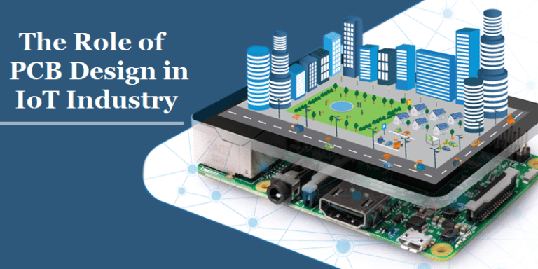
Designing a PCB for IoT applications is a complex and challenging task that requires careful planning, attention to detail, and a deep understanding of both the application requirements and the principles of PCB design.By following this step-by-step approach, you can create a PCB that not only meets the functional needs of your IoT device but also ensures reliability, scalability, and efficiency. IoT Design: Basic Building Blocks. At its core, an IoT device has a couple of key components that define it: sensors, a wireless connectivity block, and a power management block. The main challenge in successful IoT design is having them all work together smoothly. Sensors. Firstly, sensors focus on gathering data from the outside world.
Designing PCBs for Embedded Systems and Internet of Things Circuit Diagram
In this comprehensive video, Peter from Tech Explorations takes you through the entire process of designing a custom IoT PCB using KiCad 9. From schematic cr
Complete step-by-step PCB design process going through the schematic, layout, and routing of a ESP32-based PCB including USB in the new KiCAD 7. All the way